Co-designed, co-built, and co-characterised a 50 W Dual Active Bridge (DAB) DC-DC converter. The project spanned four sequential reports: converter sizing and PLECS simulation, magnetic component design and construction, full schematic and PCB layout in Altium, and finally physical assembly, digital control implementation, and efficiency measurements on the bench.
DAB DC-DC Converter: Full Design Cycle
Objective
Key Contributions
- Converter Sizing & Simulation (R1): Derived all main component values analytically for a 50 W / 24 V output DAB operating at 250 kHz. This included the transformer turn ratio, series inductor, phase-shift range, output and input capacitances, and DC-blocking capacitor. Validated output voltage ripple, MOSFET current waveforms, and thermal margins in PLECS across the full input voltage range (30-60 V) and down to 25% of nominal power. Selected primary and secondary side MOSFETs based on voltage/current stress calculations and computed conduction and switching losses together with heatsink requirements.
- Magnetic Component Design & Construction (R2): Sized the high-frequency transformer from core loss budget through the Kgfe method: determined volt-second stress, selected peak flux density, computed required turns, and verified the turn ratio for both output and auxiliary ports. Designed the winding window allocation and selected wire gauges accounting for skin depth at 250 kHz. Built the transformer prototype and verified it with LCR meter and frequency-response analyser tests (open-circuit, short-circuit, saturation, and heat-run). Separately designed and wound the series inductor on a gapped core and measured its inductance and copper losses.
- Schematic & PCB Design (R3): Completed the full Altium schematic: power stage (input/output capacitors, DC-blocking cap, discharge resistor), primary and secondary bootstrap gate drivers with VDD decoupling and gate resistor sizing, inductor over-current protection circuit, current-sensing with shunt resistors and INA201 amplifiers, resistive voltage dividers with op-amp followers, and auxiliary 12 V / 3.3 V LDO supply chains on both galvanically isolated sides. Created custom footprints, generated the BOM, and laid out the PCB with minimum copper-width rules enforced for all high-current tracks.
- Assembly, Digital Control & Testing (R4): Implemented a PI output voltage controller in PLECS using code generation onto a TI F28335 DSP. Tuned gains in simulation, added soft-start and dead-time logic, and validated all protection paths before powering up the converter. Followed a structured testing sequence: verifying auxiliary supplies, sensing circuits, gate-driver waveforms, and MOSFET switching on each side independently before connecting both bridges. Ran open-loop and closed-loop tests at the nominal operating point, and captured a full efficiency curve using a power analyser and thermal camera.

Visuals
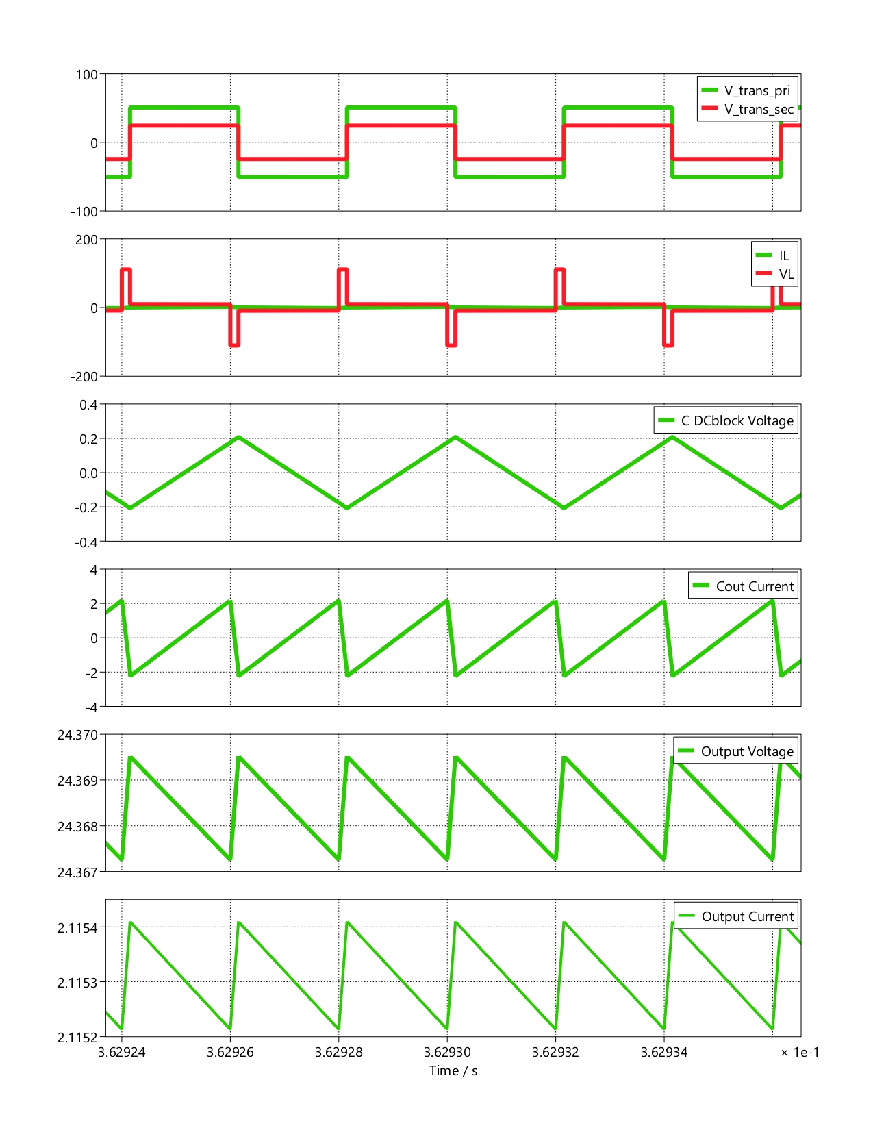 Fig 1. PLECS simulation: transformer voltages, inductor voltage and current, DC-blocking capacitor voltage, output capacitor current, and output voltage at maximum input voltage (V_in = 60 V, φ = 0.24 rad)
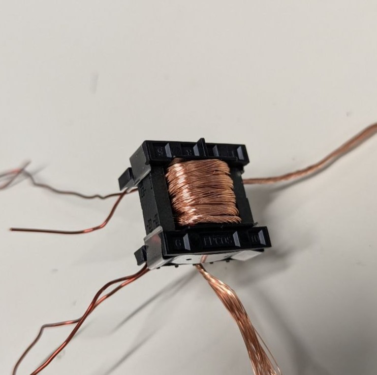 Fig 2. Hand-wound HF transformer prototype with custom wire selection and core
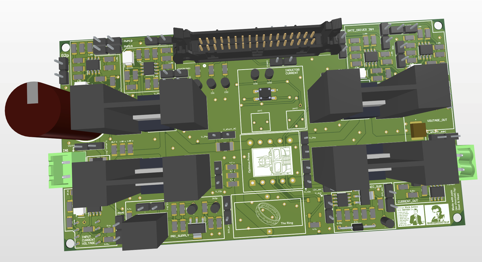 Fig 3. 3d view of the PCB layout (Top view)
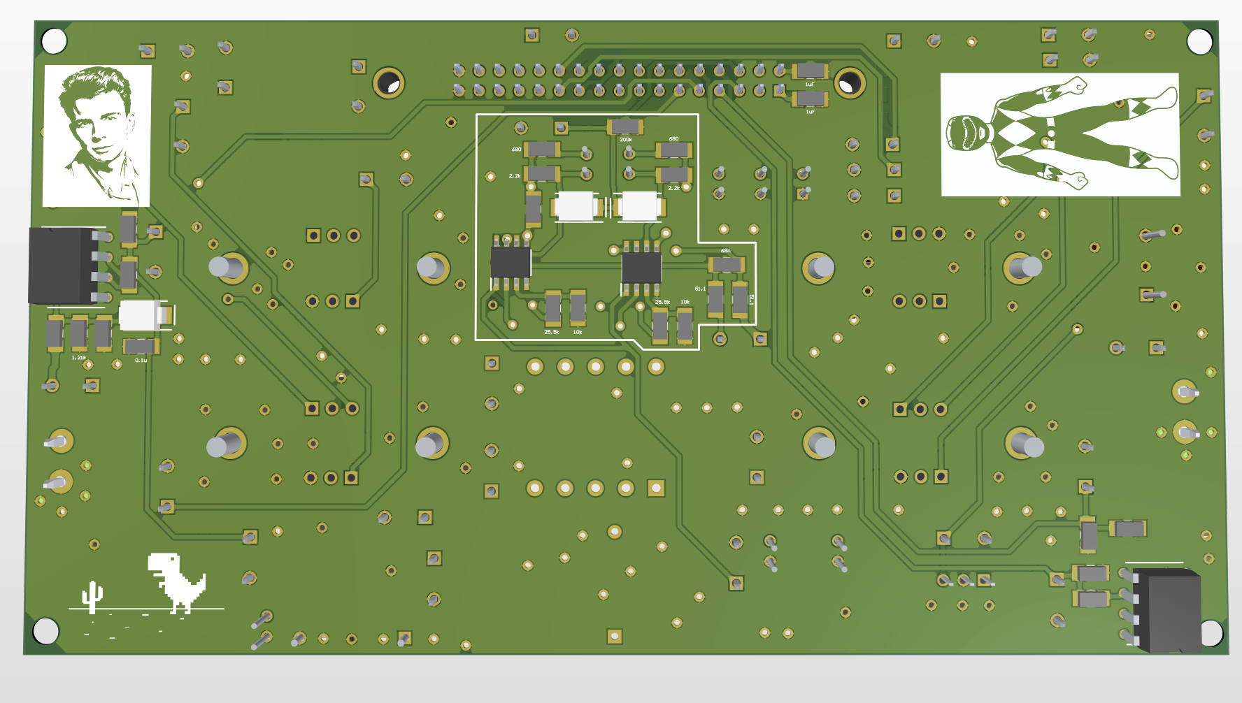 Fig 4. 3d view of the PCB layout (Bottom view)
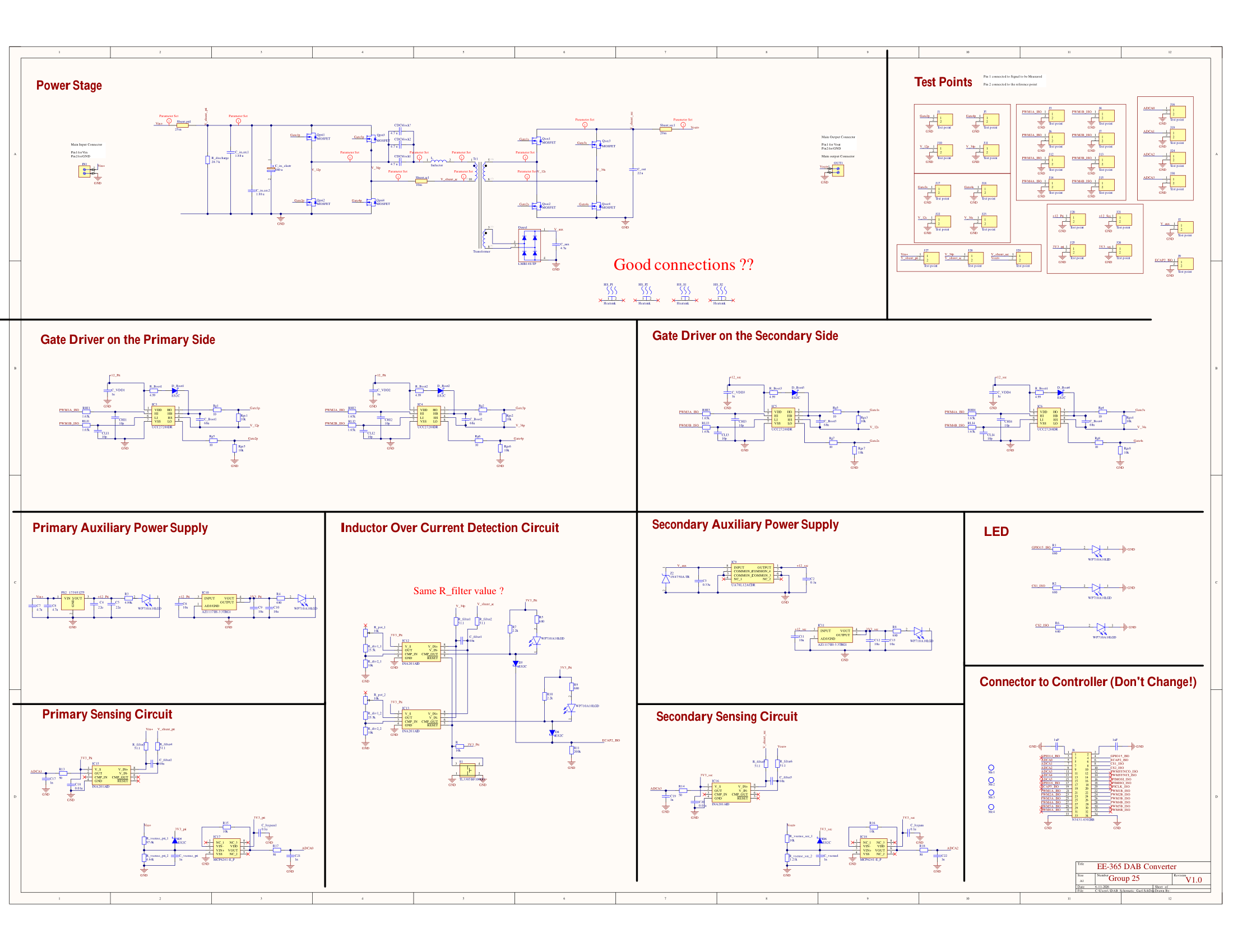 Fig 5. Full Altium schematic: power stage, gate drivers, sensing, and auxiliary supply chains
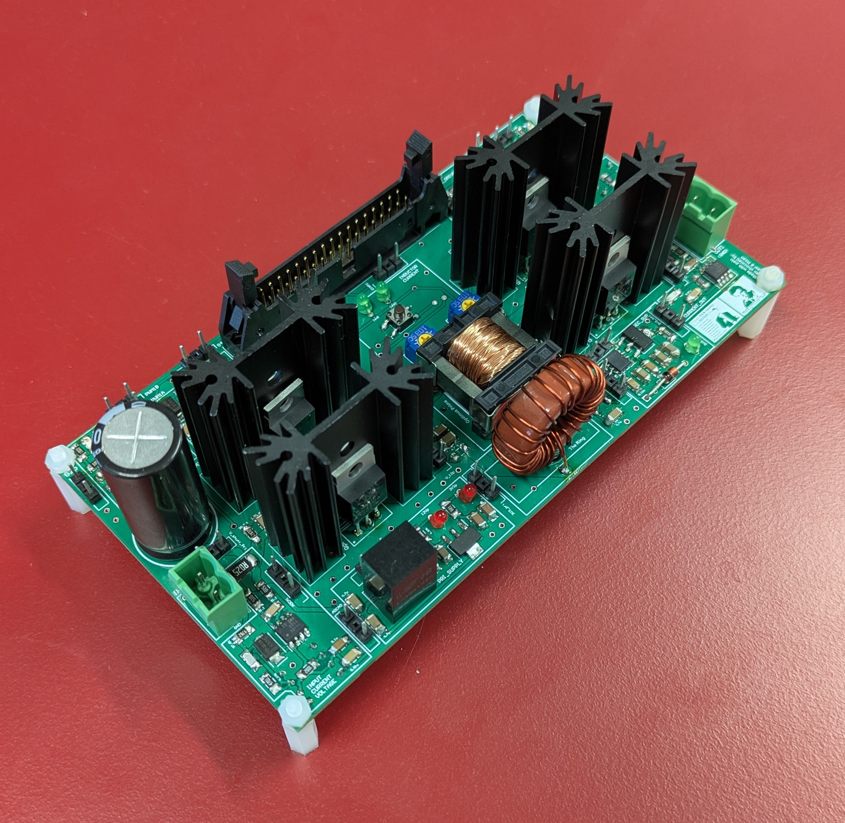 Fig 6. Assembled converter
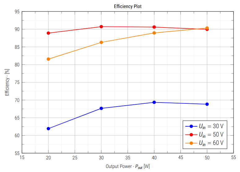 Fig 7. Measured efficiency curve across output power range
Fig 1. PLECS simulation: transformer voltages, inductor voltage and current, DC-blocking capacitor voltage, output capacitor current, and output voltage at maximum input voltage (V_in = 60 V, φ = 0.24 rad)
Fig 2. Hand-wound HF transformer prototype with custom wire selection and core
Fig 3. 3d view of the PCB layout (Top view)
Fig 4. 3d view of the PCB layout (Bottom view)
Fig 5. Full Altium schematic: power stage, gate drivers, sensing, and auxiliary supply chains
Fig 6. Assembled converter
Fig 7. Measured efficiency curve across output power range